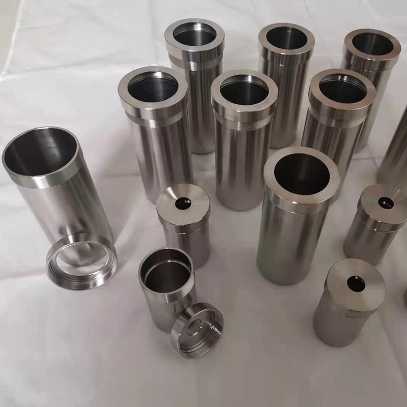
The source material for preparing sputtered thin films, also known as sputtering targets, especially high-purity sputtering targets used in physical vapor deposition (PVD) process in electronic component manufacturing, is a key material for preparing electronic thin films on the surface of wafers, panels, solar cells.
In a vacuum, accelerated ions are used to bombard the surface of a solid. The ions exchange momentum with the atoms on the surface of the solid causing the surface atoms of the solid to leave the solid and deposit on the surface of the substrate to form the desired thin film. This process is called sput. The solid that is bombarded is the source material for depositing thin films by sputtering, and is usually called the target material
Sputtering targets are mainly composed of target blanks and backing plates. Among these, the target blank is the material targeted by the high ion beam and is the core part of the sputtering target. During the sputtering process, the target blank is bombarded by ions, causing its atoms to scatter and deposit on the substrate to form an electronic film. Since high-purity metals have low strength, and sputtering targets need to be installed dedicated equipment to complete the sputtering process, the internal environment of the equipment is high voltage and high vacuum. Therefore, ultra-high purity metal sputtering need to be joined with backing plates through different welding techniques (commonly known in the industry as bonding technology) to ensure the target can be securely fixed. Additionally the backing plate needs to have good electrical and thermal conductivity.
